ABSTRACT. Low-silver and no-silver lead-free PCB solder alloys represent substantial cost savings over SAC alloys that contain 3% silver. Many wave solder operations use silver-free alloys for through hole soldering, and SMT operations are also beginning to adopt the alloy for surface mount soldering.
This paper reviews two case studies that test Ni-modified SnCu solder paste on mixed technology circuit assemblies which currently use SAC305 in production. The major differentiator between the two cases is the reflow profile: In one case, the SAC profile was considered nearly perfect for the SnCuNi alloy, peaking at 245°C. In the other case, thermally sensitive components constrained the profiles to peaking near 235°C, only 8 degrees above the silver-free alloy’s 227°C melting temperature. This important case is used to explore the lower limit of reflow capability and compare it against the baseline provided by the typical thermal process.
The performance of the solder pastes and joint formation in both cases are evaluated using numerous assembly metrics and reliability tests, including visual and automatic optical inspection, X-ray inspection, in-circuit and functional testing, optical microscopy, thermal aging, thermal cycling and shear testing. The results are presented and discussed.
Key words: Lead-free solder paste, silver-free solder paste, Sn100C, Ni-modified SnCu
INTRODUCTION. Nickel-modified SnCu, also known as SN100C®, is a commonly used lead-free electronic solder alloy. Its predominant application is in wave soldering, because it offers numerous advantages over SAC305, including much lower copper dissolution rates1, smoother and shinier solder joint surfaces without shrinkage cracks, and considerably lower cost due to the elimination of the silver content.
It is not as commonly used as an SMT alloy, however, due in part to its slightly higher melting temperature in comparison to SAC305. The non-eutectic SAC305 alloy has a solidus temperature of 217°C, a 3-4 degree pasty range, and liquidus temperature between 220 and 221°C. Eutectic SnCuNi is completely liquid at 227°C, only 6-7 degrees higher than SAC 305.
Recommended peak temperatures in reflow processes are usually 12-30 degrees higher than the solder alloy’s melting temperature. Peaking reflow temperatures within 10 degrees of a solder’s liquidus point can prompt concerns about solder joint quality and integrity. Wetting speeds and intermetallic formation rates are slower at lower temperatures, introducing the potential to create “cold,” poorly wetted, or otherwise inferior and perhaps unreliable solder joints. The capability of the SnCuNi solder alloy and flux to form quality interconnections on the low end of the reflow process window is tested by running it in a production process and comparing it with SAC305 in the same process, and with both alloys reflowed in a hotter process.
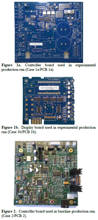
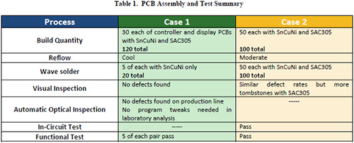
PCB ASSEMBLY: Test Vehicles. The test vehicles used in these experiments are shown in figures 1a through 2. PCBs 1a and 2 are both industrial controller boards, measuring approximately 6x6” and 8x8” respectively. PCB 1b is a display board that accompanies PCB 1a, and measures approximately 3x3.5.”
Assembly Processes. PCBs 1a and 1b were printed using Type 4 AIM NC259 solder paste for both alloys with 0.005” electroformed stencils for both assemblies on an EKRA X4 printer. Components were placed with ASM SIPLACE D4 and reflowed in a 7-zone BTU Pyramax oven. 30 of each assembly were run on the production line with both SAC305 and SnCuNi solder pastes. Five of each set were assembled with PTH components and wave soldered using SnCuNi.
PCB 2 was printed using Type 3 AIM NC254 no-clean solder paste for both alloys with a 0.005” laser-cut, electropolished stencil on an MPM UP2000 printer. Components were placed with a Mydata MY12 and the boards were reflowed with a 10-zone Electrovert Omniflo oven. 50 of each assembly were run on the production line with both SAC305 and SnCuNi solder pastes. They were all fully assembled with PTH components and wave soldered with SAC305 or SnCuNi, corresponding to their SMT solder alloy.
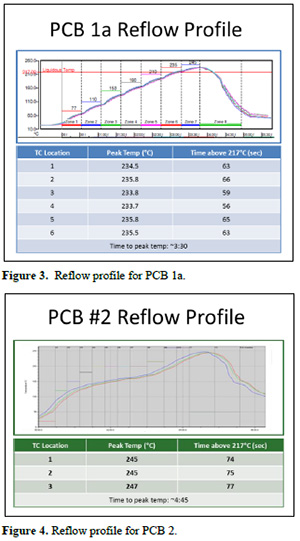
Reflow Profiles. PCBs 1a and 1b ran relatively fast, cool, ramp-style reflow profiles, reaching peak temperatures of 233-236°C in about 3 minutes 30 seconds, with 55-65 seconds above 217°C (figure 3) . In contrast, PCB #2 ran a longer, hotter, soak-style profile that peaked at 245°C in 4 minutes 45 seconds (figure 4).
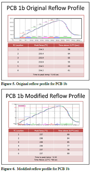
Visual inspection of PCB 1b on its original reflow profile indicated minimal wetting to some of the SOIC leads and a few unmelted solder spheres near areas of higher thermal mass. Maintaining considerations for the thermally sensitive component(s), the profile was modified slightly by slowing the conveyor and increasing one zone temperature. These changes raised the peak temperature to 237°C with an approximate time above 227°C of 60 seconds and demonstrated improved wetting upon visual inspection. The original and modified profiles for PCB 1b are shown in figures 5 and 6.
INSPECTION & TEST: Assemblies 1a and 1b. All 120 PCBAs were inspected with a Mirtec MV-7 Automated Optical Inspection immediately following reflow. No defects were identified. They were also 100% visually inspected by certified inspectors, with no defects found. 5 of each set of PCBs (SAC305 and SnCuNi) were fully built up with PTH components, wave soldered (all with SnCuNi) and assembled into chassis for functional test. All passed.
Assembly 2. All 100 PCBAs were visually inspected, in-circuit and functionally tested. Defect rates were similar with the exception of tombstones. This PCB design has a propensity for tombstoning in its usual production process. In this build, the SAC305 assemblies averaged 3 tombstones per board, whereas the SnCuNi assemblies had no tombstones at all.2
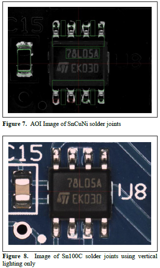
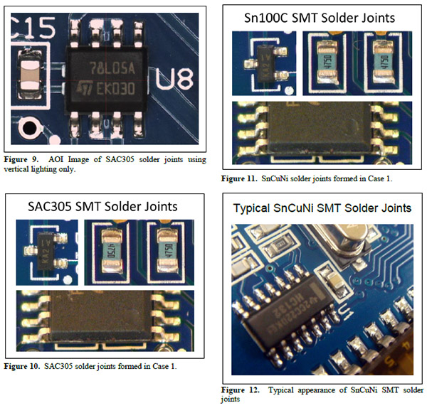
ADDITIONAL AOI TESTING. Samples of PCBAs 1a and 1b were submitted to Mirtec for additional AOI compatibility analysis. Using the MV-3L AOI system’s standard H-V light algorithm (figure 7) very little difference in the reflectivity of the joints was noted. Minor differences were noted when using non-standard horizontal or vertical lighting only (figures 8 and 9).
Using standard solder joint identification and inspection algorithms, the AOI systems processed both alloys without requiring any changes to the standard inspection parameters.
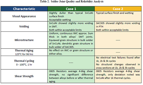
SOLDER JOINT ANALYSIS: Visual Appearance. In addition to the professional visual inspection on the assembly line, samples from Case 1 were again inspected photodocumented. Figure 10 shows examples of the SAC305 SMT solder joints and figure 11 shows examples of the same joints formed with the Ni-modified SnCu. While the SnCuNi joints are shinier and smoother than the SAC305 joints, they do not exhibit the typical luster associated with this alloy (figure 12), presumably due to their low thermal exposure during the liquidus phase of the reflow process. Despite their relatively lackluster appearance, they exhibit acceptable wetting throughout the PCB assembly, including areas of higher thermal mass.
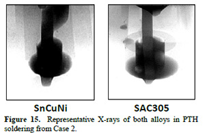
X-Ray. Both SMT and PTH solder joints were inspected by manually operated transmission X-ray. Case 1a was chosen for SMT because the fastest, coolest reflow profile offers the greatest opportunity for voiding. Case 2 was chosen for PTH to allow a performance comparison of the two alloys in wave soldering. Representative X-rays are shown in figures 13-15.
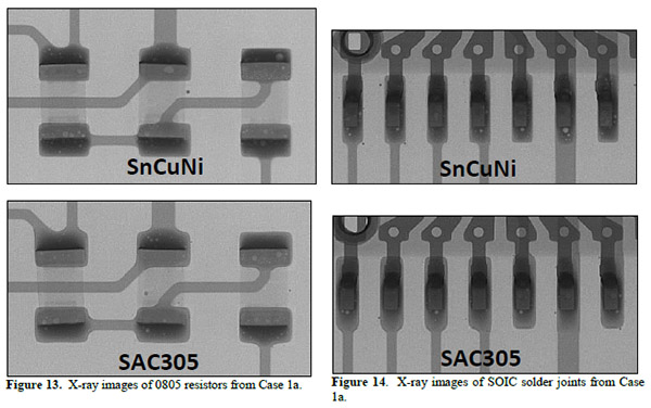
Both solder alloys demonstrated some degree of voiding in the SMT solder joints, but well below the 25% guideline for acceptability. The Ni-modified SnCu alloy showed slightly more voiding in the SMT solder joints of Case 1; the SAC305 showed slightly more voiding in the PTH solder joints of Case 2. It is believed that the level of SMT voiding seen in Case 1 can be reduced by reflow profile modifications that add some soak time in the ramp phase to permit outgassing of volatiles without increasing the ramp rate, peak temperature or TAL dictated by the boards’ temperature-sensitive components. The level of voiding in Case 2’s PTH components is not addressed because wave soldering of can have varied and multiple causes of voiding, including materials and processes used in PCB fabrication, component manufacturing or PCB assembly.
Microstructural Analysis. Samples from Case 1a, which is the fastest, coolest profile that offers the least opportunity for wetting and intermetallic compound (IMC) formation, were cross-sectioned and examined via optical microscopy.
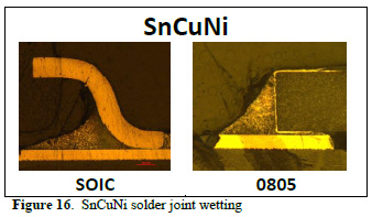
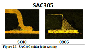
Figures 16 and 17 show good solder wetting to gull-wing and end-terminated components for both SnCuNi and SAC305.
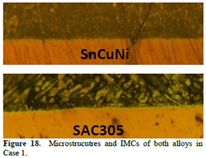
The SnCuNi joint shown in figure 18 has a continuous, uniform IMC approximately 3um thick. The IMC has a smoother, more nodular appearance due to the nickel that inhibits intermetallic growth. The SAC305 joint also shown in figure 18 also has a continuous IMC approximately 3um thick, but with a more dendritic morphology, possibly complicated by a Ag3Sn IMC formation. The SnCuNi bulk solder showed a more equiaxed grain structure, whereas the SAC305 showed a columnar grain structure.
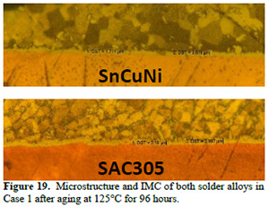
Thermal Aging. The assemblies from Case 1 were aged at 125°C for 96 hours. They were again cross-sectioned and examined via optical microscopy. The grain structures and IMCs are shown in figure 19. Thermal aging had no significant effect on IMC growth.
Thermal Cycling. Samples from Case 2, the more complex and densely populated assembly, were thermally cycled from 0 to +100°C for one hour cycles. After each 1000 cycles, they were in-circuit and functionally tested. Grain structure and shear strength were also assessed. This process was repeated three times, for a total of 3000 thermal cycles. No solder-related defects were found on any of the assemblies during any of the electrical testing. No structural changes were observed in any of the cross sectioned solder joints.
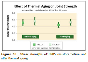
Shear Tests. Samples from both cases were shear tested. 0805 chip resistors were sheared at 15° angles on a Dage 4000 series shear tester. In Case 1, 16 of each component were tested before thermal aging and 8 of each after. No appreciable differences were noted in overall shear strength, which ranged from 4-6kg, as expected. SAC305 demonstrated slightly higher average shear strength, with slightly larger standard deviations than SnCuNi. The results are shown in figure 20.
In Case 2, 10 components were tested after each of 1000, 2000 and 3000 thermal cycles. Most of the results were also in the anticipated 4-6kg range, with the exception of the SnCuNi at 1000 cycles, which averaged only 3.1 kg (figure 21). The root cause of the low values and small standard deviation in this dataset is unknown. The remaining tests at 2000 and 3000 cycles produced results in the expected ranges.
PCB ASSEMBLY AND ANALYSIS SUMMARY. The assembly and test process is summarized in table 1; the solder joint quality and reliability analysis is summarized in table 2.
DISCUSSION AND CONCLUSIONS. Ni-modified SnCu solder alloy should be considered a viable replacement for SAC305 in nearly every SMT assembly process. The tests in Case 1 reflowed the SAC alternative in a profile that peaked at 235°C with only 60 seconds above 217°C – a thermal excursion considered near the lower limit for SAC305 processing. This profile allowed only 50 seconds above the 227°C melting point of SnCuNi. Even in a reflow process previously considered too cool for the silver-free alloy, acceptable solder joints were formed.
The visual appearance of the SnCuNi solder joints was a bit duller than typical SMT solder joints formed with this alloy at higher peak temperatures, but good wetting and IMC formation was confirmed by visual inspection and cross-sectional optical microscopy. AOI algorithms recognized the SnCuNi solder joints using the same inspection parameters as the SAC305 joints. No program changes or tweaks were required to inspect the substituted solder alloy.
The Ni-modified SnCu SMT solder joints processed on the cooler profile demonstrated higher levels of voiding than the SAC305 solder joints processed under the same profile. Both solder pastes used the same flux. Although the level of voiding is considered acceptable, minor reflow modifications can likely reduce the incidence of voids in both alloys.
Solder joint strength was measured by shear testing 0805s. Their strength was in the normal range, and was not affected by thermal aging. Joint strength of the SnCuNi was comparable to the SAC305 formed under the same profile and also comparable to the joint strength of both alloys formed under the hotter, more traditional profile.
Thermal cycling did not affect the electrical or mechanical integrity of the solder joints in Case 2, which factored into the decision to forego the thermal cycling tests for Case 1. The solder joints formed in Case 1 under the cooler profile all exhibited typical characteristics – joint wetting, IMC formation and strength – indicative of quality, reliable solder joint formation. Originally, a planned thermal cycling test for Case 1 included cross sectioning, shear testing and electrical testing at the end of the 3000 cycles. However, given the normal characteristics of the solder joints and the abundance of thermal cycling results available on these alloys3, it was highly likely that no joints would fail and no advances in valuable knowledge would be gained by performing the tests. Therefore, they were omitted from the final analysis.
Silver-free, lead-free electronic solder alloys offer substantial cost savings over silver-containing ones, reducing solder paste costs by as much as 20 percent. This potential savings is very attractive to many OEM and CEMs, particularly in price-competitive sectors such as consumer electronics, but concerns over compatibility with the established SAC305 reflow window have slowed its implementation. Case 1 provides crucial information about the Ni-modified SnCu alloy’s reflow capability in the low end of the SAC reflow process. It demonstrates that the SN100C® can form quality, reliable SMT solder joints even in thermal profiles on the lower margin of the SAC305 process window, and should be considered a drop in replacement for nearly any SMT assembly process that uses SAC or SAC-based solder.
ACKNOWLEDGEMENTS
The authors would to thank Mirtec’s Brian D’Amico and Robert Horowitz for their AOI analysis in support of this project.
REFERENCES
[1] C. Hamilton, P. Snugovsky, PhD, Celestica, M. Kelly, IBM “A Study of Copper Dissolution during Pb-free PTH Rework using a Thermally Massive Test Vehicle,” Proceedings of SMTA International, September 2006
[2] K. Seelig, “Lead-Free Alloy Development, Proceedings of the International Conference on Soldering and Reliability, May, 2012
[3] J. Arnold, N. Blattau, and C. Hilllman, DfR Solutions, K. Sweatman, Nihon Superior, “Reliability Testing of Ni-Modified SNCu and SAC305 – Accelerated Thermal Cycling,” Proceedings of SMTA International, October, 2008
Additional reference material includes internal reports from Shea Engineering Services titled “Hayward Build Report April 30, 2013” and “Hayward PCB Assembly Images Report” issued April 17, 2013, available upon request from AIM Solder.


