Technical Articles

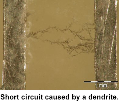
ABSTRACT  Implementation of low-temperature solders has been a subject of considerable interest for many consumer electronics manufacturers. Low-temperature solders represent a significant material and process cost advantage over traditional silver-bearing and low-silver alloys. Bismuth-containing alloys enable low-melting temperatures; therefore, if the mission profile of an assembly tolerates the limitations of bismuth-containing low-temperature solders, implementation is favorable. 

An overlooked application in implementing low-temperature alloys is rework. The inherent brittleness of bismuth inhibits the manufacturing of fluxed cored wire. An approach to overcome this limitation is to use a high- bismuth solid wire solder with an external flux. This approach introduces challenges associated with implementing new materials and training operators on new rework techniques. Another approach is to use traditional tin (Sn)/ silver (Ag)/ copper (Cu) (SAC) flux cored wire solder to...

Can a change of solvent in the printer improve SMT printing?

ANY ENGINEER WILL TESTIFY lab testing may not correlate with field results. Laboratory data are developed under ideal conditions to generate accurate and repeatable data, whereas a production setting introduces variables not reproducible in the lab environment.

In this report, AIM’s application lab approximated a production environment in a multi-hour printing test to quantify the effect of under-stencil wipe solvent on solder paste performance. This experiment compared isopropyl alcohol (IPA) and a novel stencil cleaner. IPA is not recommended as an in-process stencil cleaner, but is often used because it is inexpensive, effective and readily available. However, IPA is not a constituent of solder pastes and can therefore cause changes to paste that will negatively impact performance.

One example of this change is that paste exposed to IPA can become...

With no standard in sight, emerging alloys require unique fluxes and processes.

LOW-TEMPERATURE SOLDERING is a subject of considerable interest and development. Several forces are driving implementation of solders with lower peak reflow temperatures than SAC 305 and its variants. The most technically significant is reduced warping of component and substrates. Chip suppliers are particularly interested in lower reflow temperatures, as thinner components are needed to meet dimensional limitations of thinner, smaller and faster devices. When a component deforms during reflow, the solder interconnect may be compromised, resulting in non-wet opens (NWO). NWO defects are difficult to detect and may not manifest until after a product is in the field. Other advantages of low-temperature soldering include the incorporation of lower-cost plastics, component and laminate materials, and reduced energy consumption and related environmental...

Could vendor collaboration get to the root cause of an intermittent soldering problem?

Simply put, the ultimate function of a PCB assembly line is to create millions of solder joints without error. This task is complicated by the myriad materials that come together during assembly, and relies on the quality of each lead, pad and sphere to be soldered. When a soldering defect is discovered, it is common practice to presume the soldering materials are the cause, which seems logical, considering it is a solder defect. This assumption is often misplaced. This scenario plays out regularly, as illustrated in a recent case submitted to our failure analysis team for diagnosis.

In this case, the assembler had an intermittent solderability issue with a component. It brought the problem to its local representative’s attention on several occasions. The issue was...

Is reflow the only process where the outcome could be impacted in real-time?

One of AIM’s field engineers came back from a cross-country trip this week with stories of a profiling issue that was giving the client difficulties. Ultimately, the issue was design-related with a large ΔT that could not be overcome with the equipment used in production. It took a full day of attempts to make that final assessment. 

Many engineers and technicians I work with rank reflow profiling alongside getting their teeth cleaned or an early morning workout. You know you need to do it, and the benefits are significant, but they aren’t immediate, and it is an unpleasant chore. Let’s take a minute to go over best practices for reflow profiling. Ideally, a “golden board” will have been supplied as part of the work kit by your customer or your design team. This...

Picking the right tool to prevent electrochemical contaimination at the rework bench.

A half-dozen versions of the same scenario occurred in the past month, all having to do with materials and processes used in post-op/rework applications. This step of the production process often escapes the attention of engineers because there’s no cool machinery or any real engineering that takes place. Most hand-solder operators are highly proficient and have developed techniques that get the job done, which can lull a supervisor or production manager into a false sense of...

With RoHS exemptions set to expire, can SAC305 hang on?

It is not the strongest of the species that survive, nor the most intelligent, but the one most responsive to change.
– Charles Darwin

The final steps of RoHS will be phased in over the next 24 months and once implemented; lead will be virtually eliminated from the solder supply chain for electronic assembly. With the last exemptions applying predominantly to high reliability applications, the materials in use are being scrutinized to determine if they can perform to the mission requirements of high reliability PCB. Concurrent to this material concern, is the unrelenting trend in...

With RoHS exemptions set to expire, the SMT market might see a host of new solders.

I vividly remember a moment in 1994, sitting in a job interview, trying to conjure an image of the periodic table for the abbreviations for tin (Sn) and lead (Pb). Of course, these weren’t easy guesses because both elements’ abbreviations are derived from their Latin roots: tin from stannum and lead from plumbum. I incorrectly provided my interviewer with the abbreviation for titanium (Ti) and the famously nonexistent unobtainium (Uo). As confused as I was at the time, little did I realize how simple things actually were.

Back then, there was essentially one alloy in use for electronics assembly: Sn63/Pb37. A few specialized applications used a small percentage of silver (Ag) in the SnPb, tin-silver or high-lead solders, and a handful of old-timers wouldn’...

Stop Tweaking the Ground Pad Prints; Start Tweaking the I/O Prints.

Would you believe QFN ground pad voids could be cut by over 50% with a zero-cost, super-simple stencil aperture modification? Not a mod to the ground pad apertures where the voiding is problematic, just to the I/O apertures? Neither did we. That’s why we did some deeper digging into what we are now calling the “AIM I/O” aperture modification before introducing it.

On the Tech Tips, we reported a dramatic reduction in voids when QFN I/O pads were left unpasted, but doesn’t stop there, that observation lead and experimentation lead us to an effective and repeatable void reduction technique, but we didn’t tell you exactly what that I...

Sometimes the answers to the most tenacious questions are right under your nose.

As I sit in Chicago’s O’Hare Airport having just left another productive and exciting SMTA International trade show, I reflect on what an excellent opportunity this event presents to network and stay current in the world of electronics assembly. If you don’t attend these events regularly, you should. I was fortunate to have the opportunity to attend a number of the technical conference sessions and not only learn what is emerging, but also speak with customers and colleagues on what they see as the most pressing needs of the market.

To sum it up… BTC void reduction. The technical sessions on void reduction I attended were all standing room only, and the topic was the subject of many hallway conversations among technologists. The presentations offered supplier and user...

STENCILS: Coated vs. Uncoated... what’s better for the process?

We’ve been doing a lot of print testing in our lab. In our first set of published results, “The Impact of Reduced Solder Alloy Powder Size on Solder Paste Print Performance” from IPC/APEX, we revealed a hierarchy of input variables to maximize solder paste transfer efficiency and minimize variation. In that study, we used a fully-optioned stencil as part of the equipment set. In order to tease out the data we were looking for, we could not lose critical information to the noise of stencil-induced variations.

If the stencil in that study were an automobile, it would be a Bentley. It was made by a consistently top-...

Abstract

From the Apple™ Watch and body cameras for law enforcement to virtual reality hardware and autonomous transportation, the demands and opportunities for electronics to improve our lives are only limited by our imagination. The capability of existing PCB assembly technology needs to advance rapidly to meet the mission profile of these new devices. The demand common to all of these devices is increased functionality in a smaller space. For the solder paste manufacturer, this path inevitably leads to incorporating finer metal powder into solder paste to facilitate ultra-fine pitch printing. In this study, we will evaluate the benefits and implications of finer mesh solder powder on critical aspects of solder paste performance. 

Type IV, V, VI SAC305 solder powder will be tested and their characteristics in several key areas will be measured and studied. The key variables will be print...

Stencil printing is efficient and effective, but it is not without its limitations.

Stencil printing is an efficient and effective way of applying millions of well-controlled solder paste deposits, but it is not without its limitations. Many packages, such as area array and bottom termination components, keep getting smaller, while connectors, shields and other big components remain the same size, or grow even larger. Pushing the limits of stencil printing on either or both ends of the printable size spectrum can present considerable challenges for PCB assemblers.

One way to conquer these challenges is to dispense solder paste. Dispensing is an attractive option because it allows for infinite flexibility - it can produce both very small deposits or large deposits and it is fully compatible with the existing SMT process and materials. In fact, many...

Or what the @#$% is a squircle, and what is it doing on my stencil?

The term “squircle” is a portmanteau, or mashup, of square and circle. It’s a real word, and the shape is also known as a superellipse to supernerds. We jest, but besides having a funny name, the squircle is an effective tool for maximizing solder paste release and overall deposit volume.

A squircle (FIGURE 1) is a square with rounded corners that, when incorporated into stencil aperture designs for small area arrays, provides better print quality than either a square or a circle alone. It brings the best of both worlds to an extremely challenging part of the printing process.

...

Paste viscosity can inform why solder performs differently under different conditions. 

Viscosity and thixotropy are not words heard in casual conversation, yet they are very common material characteristics we encounter in our everyday lives.

Viscosity is defined as a fluid’s resistance to flow, but is more commonly referred to as a fluid’s “thickness” (flowing slowly like motor oil) or “thinness” (flowing easily, like water). Thixotropy, on the other hand, is a unique property in which viscosity changes with the forces being applied to...

Proper handling and storage controls go a long way toward print quality.

Solder paste is an elaborate mixture of metal powders, acids, thixotropes, solvents and a variety of other chemicals. When combined, the reactions and interactions can be extremely varied and complex. When designing solder paste chemistry, key considerations include not only its inprocess performance but how to maintain the stability of that performance against the rigors of time, temperature fluctuations and usage. 

Stencil printing is arguably the critical process on the assembly line because it lays the foundation for the entire assembly. A quality print does not necessarily preclude rework, but a bad print effectively guarantees it. Additionally, the PCB assembly process is vulnerable to external influences, such as operating environments, setup changes and operator...

In Search of the Perfect Solder Paste. Hint, it's a moving target.

Solder paste – that ubiquitous, viscous, sticky blob that is applied as the first step of every SMT assembly process – is a surprisingly complex product. It is composed of two primary constituents: solder powder, which accounts for 85% to 90% by weight or 50% by volume, and flux medium as the balance. As complicated as powder development and manufacturing can be, flux medium is even more so, due to the myriad demands and constraints placed on it.

Imagine you are planning a big party and you decide to make the aptly named Patience Cake (FIGURE 1) – arguably one of the most complicated baked goods recipes imaginable. Different batches of batter must be mixed in advance, refrigerated overnight and baked in individual pans. Pieces of the baked goods are then precision cut, and evenly...

Comparing Properties of CASTIN™, BABBITT & Alternative Lead-Free Alloys

Abstract.  This paper compares three commercial lead-free solders; CASTIN®, Babbitt and SAC-I and their modified compositions in terms of mechanical and soldering properties. Solders tested are six alloys with different compositions in the range of (major elements): Sn/Cu(0.7-4)/Ag(0-4)/Sb(0.5-8)/Bi(0-3)/Ni(0-0.15). Effects of alloying elements on the thermal behavior (melting and solidification), wetting force, contact angle, spreading, tensile and hardness properties are studied. Based on preliminary results an alloy modification is made and its properties are compared and discussed against the commercial creep resistant solder alloy, i.e. SAC-I.

Key words:
Lead free solder, wetting, mechanical properties, thermal behavior

...

A finer type solder paste may solve one problem only to create another.

From Univac to the latest wearable gadget, electronics keep shrinking. As transistors get smaller, so too do their packaging, solder interconnections, and a key ingredient in making those interconnections: solder powder. Often overlooked on miniaturization roadmaps, the ultrafine particles of metal carried in solder paste play a critical role in solder joint formation, and must be optimized for printing and reflow of subminiature solder joints.

The solder powder manufacturing process is very complex and involves atomizing molten alloy and solidifying the tiny droplets while dispersed in gas. There are many different ways to atomize metallic powders. Most methods are considered proprietary and are rarely discussed in public forums. A solder paste’s flux and its attributes garner a...

To err is human; to blame the other vendor is… policy.

Nearly every process engineer has found themselves in this quandary: something goes awry with the process, and the supplier finger-pointing begins immediately. With machines, chemistry, components and PCBs all factoring into the mix, it often appears that a supplier’s first line of response is to deflect responsibility rather than help seek the root cause. Chemistry providers don’t have the luxury of suggesting a few mechanical measurements or a quick check under the hood to rule out our products as the source of problems, so we are accustomed to rolling up our sleeves and helping solve them.

We occasionally field calls on solder mask crazing, delaminating or peeling after wave solder. Solder mask problems are not uncommon at all, and we’ve certainly seen our share over the years. Nearly all solder mask...

Pages