- Productos
- Soldadura en pasta
- Flux líquido y en pasta
- Soldadura en alambre
- Soldadura en barra
- Aleaciones de soldadura
- Materiales de soldadura adicionales
- Libre de Halógenos
- Materiales de soldadura para la industria LED
- Materiales de soldadura para la Industria Automotriz
- Materiales de soldadura para Militar y Aeroespacial
- Servicios
- Soporte
- Hojas de Datos
- Noticias
- Contacto
- Acerca
By Karl Seelig, Vice President Technology and David Suraski, Executive Vice President
Abstract. As the electronics industry begins to focus upon the tin-silver-copper family of alloys as a viable replacement for tin-lead solders, research needs to be done to determine if any particular alloy is best suited for the broadest range of applications. The tin-silver-copper family of alloys has earned a great deal of positive response from various industry consortia and organizations in recent years and the majority of manufacturers plan on implementing one of these alloys. However, as there are several different alloy formulations within the tin-silver-copper family, background information is necessary to determine which alloy is best suited for the broadest range of applications.
Introduction. It is inevitable that lead will be eliminated from a great deal of electronics assembly. Whether this will be the result of legislation, marketing pressure, or de facto trade-barriers is not important. The only important aspect of this issue anymore is that it is real, and that it is coming within the next few years. Therefore, electronics manufacturers need to be cognizant of the solder alloy choices available to them, and the fact that not all alloys, including those within the same families, share the same characteristics.
Based on recent industry-wide developments, it appears that the choice of candidate lead-free alloys to replace tin-lead for electronics assembly is narrowing. Despite a confusing patent situation and continuing questions about reliability, the tin-silver-copper family of alloys has earned a great deal of positive response from various industry consortia and organizations in recent years and the majority of manufacturers plan on implementing one of these alloys.i In general, this family of alloys demonstrates relatively low melting points, good reliability characteristics, and, depending upon the exact composition, reasonable cost. However, as there are several different alloy formulations within the tin-silver-copper family, background information is necessary to determine which alloy is best suited for the broadest range of applications.
It also should be noted that these (sometimes nominal) varying alloy compositions are confusing to the industry and create an inventory nightmare for solder manufacturers and end-users. The result is a higher cost for the industry. Selecting a “default” lead-free alloy benefits the entire supply chain. This is especially true of EMS providers, who may be forced to stock multiple alloys based upon the requirements of their customers.
Tin-Silver-Copper Alloy Comparison. The alloys tested are the most promising and popular of the tin-silver-copper alloys: Sn96.5/Ag3.0/Cu0.5, Sn95.5/Ag3.8/Cu0.7, and Sn95.5/Ag4.0/Cu0.5. In addition the Sn96.2/Ag2.5/Cu0.8/Sb0.5 alloy is used in some cases as a low-silver content alternative for comparative purposes. This paper is meant to provide the baseline information for these alloys needed to fairly compare one to another. Objective test methodologies were used to represent key-criteria in the transition to lead-free electronics assembly. The issues that will affect the broadest range of users of these alloys are addressed in this study. Included in the comparison is availability, cost, solder paste printing, melting, wetting, wave soldering, thermal fatigue and solder joint reliability characteristics. Of course, individual companies are encouraged to perform further tests in order to determine the viability of these alloys for their particular parts, processes, and applications.
Lead-Free Alloy Element Tolerances. It should be noted that solder alloys have an acceptable tolerance for each component element. Per IPC-J-STD-006, elements that constitute up to 5% of an alloy may vary by up to ± 0.2%, while elements that constitute greater than 5% of an alloy may vary by up to ± 0.5%.
For example, the Sn63/Pb37 alloy may contain between 62.5% to 63.5% tin and 36.5% to 37.5% lead. The Sn62/Pb36/Ag2 alloy may contain between 61.5% to 62.5% tin, 35.5% to 36.5% lead and 1.8% to 2.2% silver.
Below is a chart of various lead-free solder alloy compositions and their potential elemental range. This is intended to demonstrate the likelihood of potential alloy overlap, even when specifying a “unique” alloy. This information pertains to industry standards for alloy tolerances, and not of any particular vendor.
| Alloy | Alloy Range |
| Sn96.5/Ag3.0/Cu0.5 | Sn96.0 to 97.0 / Ag2.8 to 3.2 / Cu0.3 to 0.7 |
| Sn95.5/Ag3.8/Cu0.7 | Sn95.0 to 96.0 / Ag3.6 to 4.0 / Cu0.5 to 0.9 |
| Sn95.5/Ag4.0/Cu0.5 |
Sn95.0 to 96.0 / Ag3.8 to 4.2 / Cu0.3 to 0.7
|
Alloy Availability and Patent Situation. It is desirable for the industry to find an alloy that is widely available. Therefore, patented alloys have been viewed as undesirable. However, the issue is not as simple as it seems. Manufacturers should note that certain patented alloys have been licensed to several manufacturers around the world and are widely available. Conversely, certain solder alloys that appear non-patented may not be completely free of patent coverage.
The issue of alloy patents is complex, with different alloy formulations patented in different parts of the world. In addition, what many do not realize is that most alloy patents cover not only the alloy in solder form, but completed solder joints as well.
Alloys such as Sn95.5/Ag4.0/Cu0.5 and Sn95.5/Ag3.8/Cu0.7 have been recommended to the U.S. industry despite the fact that solder joints produced from these alloys may violate patents. For one, these alloys are covered under patent in Japan, so this limits the export of products manufactured with these alloys.ii Also, it is possible that the use of these alloys could violate Iowa State University U.S. patent # 5527628. Although these alloys do not fall under this patent, these same alloys with 1.0 to 4.0 percent copper are covered. The application claim of this patent states that even a finished solder joint is covered by the patent. Therefore, if one of these non-patented alloys is used and during manufacturing the alloy “picks up” copper (which normally does occur) and forms an intermetallic that contains the elements covered under the Iowa State University patent, the manufacturer has violated that patent. Although this will be difficult to enforce, manufacturers should be aware of this potential for patent violation.
Below is a listing of the key patents for tin-silver-copper alloys:
| Alloy Elemental Range | Patent # | Patent Holder | Geographic Coverage |
| Sn/Ag3.5-7.7/Cu1-4/Bi0-10/Zn0-1 | 5527628 | Iowa State Univ. | USA |
| Sn/Ag0.05-3/Cu0.5-6 | N/A | Engelhard & Oatey | (patents expired) |
| Sn/Ag1.5-3.5/Cu0.2-2/Sb0.2-2 | 5405577 | AIM, Inc. | USA and Japan |
| Sn/Ag3-5/Cu0.5-3/Sb0-5 | 05-050286 | Senju | Japan |
Cost of Metals Comparison. As seen below, silver is the cost element in the tin-silver-copper alloys. The cost difference for the raw metals that make up Sn95.5/Ag3.0/Cu0.5 versus Sn95.5/Ag3.8/Cu0.7 and Sn95.5/Ag4.0/Cu0.5 is US$1.43/1.30 Euros and US$1.13/1.03 Euros per kilogram, respectively. This can result in dramatic cost differential for wave soldering and hand soldering operations, as the costs of metals is a key contributor to the final cost of bar solder and wire solder, and can have an impact on pricing for SMT grade solder pastes as well. As with other cost studiesiii, included for comparison purposes is the Sn96.2/Ag2.5/Cu0.8/Sb0.5 alloy, which is the least expensive of the tin-silver-copper based alloys and shows still more of a cost reduction compared to high-silver alloys. Also included for comparison purposes are the costs of metals for Sn62/Pb36/Ag2 and Sn63/Pb37, each of which are significantly less costly than the lead-free alloys being discussed.
| Alloy | Price Per Kg iv |
| Sn95.5/Ag4.0/Cu0.5 | US$10.73 / 9.12 Euros |
| Sn95.5/Ag3.8/Cu0.7 | US$10.44 / 8.87 Euros |
| Sn96.5/Ag3.0/Cu0.5 | US$9.33 / 7.93 Euros |
| Sn96.2/Ag2.5/Cu0.8/Sb0.5 | US$8.59 / 7.30 Euros |
| Sn62/Pb36/Ag2 | US$6.36 / 5.41 Euros |
Solder Paste Printing Comparison. Although previous testing has shown little differences between printing lead-free and tin/lead solder pastesv , it is useful to prove out the similarity of the printing process windows of particular leadfree solder pastes, as this is a key factor when determining the process windows and ease-of-use of various alloys. Testing was performed to mimic manufacturing requirements in order to determine the printing process windows of the Sn95.5/Ag3.0/Cu0.5, Sn95.5/Ag3.8/Cu0.7, and Sn95.5/Ag4.0/Cu0.5 alloys. Each alloy was mated with the same no-clean paste flux chemistry with the same metal load, powder micron size and viscosity.
As seen in the images to the right, very little difference is observed in the printing of pads with 12 mil gaps when using any of these alloys. All show good aperture fill, well-formed print deposits, and resist bridging.
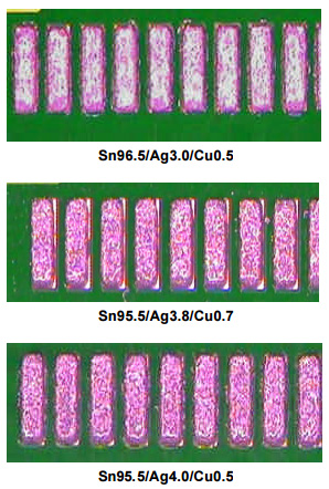
To confirm the above results, square pads with 10 mil gaps were printed using each of the three alloys on a PCB that had not had solder mask applied on it. Once again the print results were very similar and all show good aperture fill, well-formed print deposits, and resist bridging.
Furthermore, when subjected to subsequent longer-term testing, each of these pastes performed similarly.vi The testing used was performed over several hours and determined that the fine pitch printability, pause to print times, tack life, and the effect of time to solder wetting were acceptable for each of these pastes. Thus, it may be assumed that each of the tin/silver/copper alloys will provide manufacturers with a similar printing process window as tin/lead alloys.
It should be noted that successful lead-free solder paste printing characteristics does depend on if the paste manufacturer has their solder density issues resolved. Lead-free alloys are significantly less dense than tin/lead; up to 17% in some cases. If one experiences a significant difference in printing characteristics for a lead-free solder paste versus the equivalent tin/lead paste, it may be related to the metal loading or flux chemistry of the paste in use. This would typically manifest itself with a solder paste that appears very thick and difficult to print with standard squeegee pressure settings.
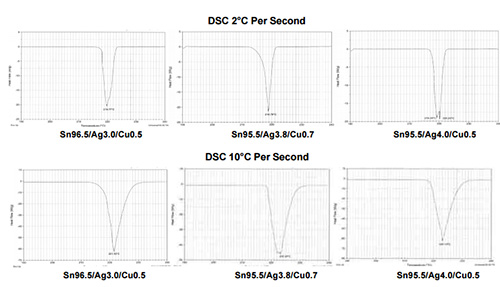
Melting Points. DSC testing was used to determine the melting points of the alloys tested. As shown in the DSC diagrams below, the melting points of the alloys tested range from 218-220°C when tested at 2°C per second, with Sn96.5/Ag3.0/Cu0.5 melting at 219.77°C, Sn95.5/Ag3.8/Cu0.7 at 218.78°C, and Sn95.5/Ag4.0/Cu0.5 at 220.23°C. When tested at 10 °C per second the melting points of the alloys remained similar, with less than 2°C separating the alloys.
Wetting. In general, lead-free alloys do not wet as well as tin-lead solder alloys. This also is true of the tin-silver-copper family. However, it is possible that different tin-silver-copper alloys will have different wetting characteristics from one another. To determine the wetting capabilities of these alloys, wetting balance testing and spread testing was performed.
Wetting Balance Testing. In wetting balance testing, the dynamic wetting force of an alloy is measured and graphed versus the time it takes to achieve wetting. In the operation of a wetting balance, the specimen is suspended from a sensitive balance and immersed edge-wise, at a predetermined and controlled rate, and to a specified depth, into the molten solder maintained at a controlled temperature. As a result of the interaction between the molten alloy and the board finish, the wetted coupon is subject to time-variant, vertical buoyancy forces and downward surface tension forces. The forces are detected by a transducer and are converted into an electrical signal, which in turn is recorded by the data acquisition system in a computer.
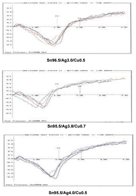
As shown above, the wetting curves from previous testing demonstrate the superiority of lowersilver tin-silver-copper alloys for wetting time and force when used with a variety of flux types. However, it should be noted that the results indicate a relative similarity between all of these alloys.
To corroborate the above, globular wetting balance testing was performed on the Sn96.5/Ag3.0/Cu0.5, Sn95.5/Ag3.8/Cu0.7, and Sn95.5/Ag4.0/Cu0.5 alloys. As shown in the graphs to the right, once again wetting time and force for each of these alloys proved similar.
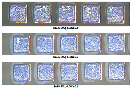
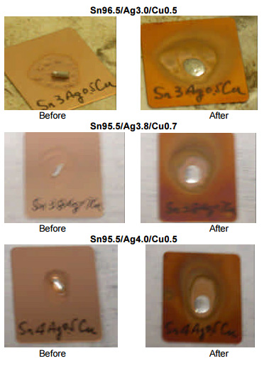
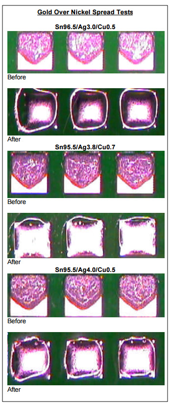
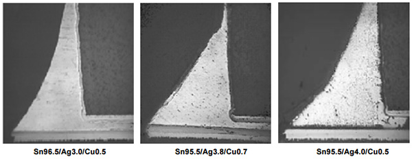
Spread Testing. Spread testing was performed as a means to gauge the wetting ability of the alloys tested. The figures below were made using the Sn95.5/Ag3.0/Cu0.5, Sn95.5/Ag3.8/Cu0.7 and Sn95.5/Ag4.0/Cu0.5 alloys mated with the same noclean paste flux chemistry. The pad material was gold over nickel and the assemblies were heated in a convection reflow oven without the use of nitrogen. As can be seen on the following page, each solder paste achieved full spread to all four edges of each pad.
In addition, spread tests were performed on test coupons heated on a hot plate. Although it may be difficult to discern from the images on the following page, spread for each sample was virtually identical and each was considered to be in the acceptable range per IPC test requirements.
From the wetting and spread tests presented here, manufacturers can expect similar wetting with each of the tin-silver-copper alloys, with slightly superior wetting likely with the lower-silver alloys.
Lead-Free Wave Soldering Considerations. While it can be tempting to concentrate solely on SMT applications when discussing lead-free soldering, it should be remembered that wave soldering continues to remain a viable and popular technology. As lead-free wave soldering becomes increasingly prevalent, questions have arisen about copper dissolution into lead-free alloys and the possibility of additional solder pot maintenance.
In a standard Sn63/Pb37 wave pot, as impurities such as copper build up, they form intermetallics with the tin. This intermetallic buildup can be systematically removed by reducing the temperature of the solder pot to 188°C (370°F) and allowing the pot to sit undisturbed for > 8 hours. The density of the Cu6Sn5 intermetallic is 8.28, while the density of Sn63/Pb37 is 8.80, allowing most of the Cu6Sn5 to float to the top of the pot after a few hours of cooling. After this the top of the pot can be skimmed and new solder added to bring up the level. This typically will maintain copper levels below 0.3% and can maintain the copper level in the 0.15% range. This is a simple gravimetric separation of Cu6Sn5.
However, the densities for tin-silver-copper alloys are approximately only 7.4. Therefore, instead of the Cu6Sn5 intermetallic floating off and easily being removed as when in Sn63/Pb37, the intermetallics sink and are dispersed through the lead-free alloy in the pot. The end result of this is copper build-up in the pot. This is also true of the Sn99.3/Cu0.7 alloy, which has a density similar to that of tin-silver-copper alloys.
The result and biggest problem of the above is that solder pots may need to be dumped more often, leading to a complete change over of the wave pot. The pot dump specification will most likely be around 1.55% copper, since above this point the alloy becomes sluggish and at 1.9 to 2% precipitation in the pot starts to occur, which can lead to damage to wave pumps and baffles. Attention should be paid to this issue when implementing lead-free wave soldering.
Solder Joint Reliability Testing. For good reason, the issue of solder joint reliability is of great concern to the potential users of lead-free alloys. How an assembly will survive after it has been soldered with a tin-silver-copper alloy must be determined before implementing an alloy for production.
It should also be understood that solder joint reliability is dependent upon several factors other than solder alloy, including solder joint geometry, fatigue severity and soldering surface finish. Furthermore, tin-silver-copper alloy fatigue resistance has been proven superior to tin/lead under certain testing condition, but inferior under other conditions. Until the failure mechanisms of the tin-silver-copper alloy systems are better understood, it is recommended to perform accelerated testing that mimics as close as possible the operating conditions of the assembly in question.
That being said, baseline comparative reliability information for the tin/silver/copper alloys being studied is important as a down-select tool. Several reports have already been published which demonstrate the thermal and mechanical reliability of these alloys.vii, viii However, few comparative tests have been performed on these alloys. Therefore, the following tests were carried out to quickly determine if there are any clear differences between these alloys in terms of reliability.
Thermal Cycling Test Results. Test boards were built using Sn96.5/Ag3.0/Cu0.5, Sn95.5/Ag3.8/Cu0.7, and Sn95.5/Ag4.0/Cu0.5 solder alloys in conjunction with 1206 thin film resistors. The boards were then thermal shocked from -40° to +125°C for 300, 400 and 500 15 minute cycles. Solder joints were then cross-sectioned and inspected for cracks.
As shown below, none of the alloys tested showed any cracks during testing up to 500 repetitions. However, it should be noted that the Sn95.5/Ag3.8/Cu0.7 and Sn95.5/Ag4.0/Cu0.5 alloys did exhibit some change in grain structure throughout the joint after the thermal shock testing, especially the latter. Further studies should be undertaken to determine whether this change of grain structure may be indicative of a potential reliability issue.
Mechanical Strength-Flex Testing. Test boards were built using Sn96.5/Ag3.0/Cu0.5, Sn95.5/Ag3.8/Cu0.7, and Sn95.5/Ag4.0/Cu0.5 solder alloys and were subjected to flex testing.ix Solder joints were then cross-sectioned and inspected for cracks. Again, the alloys tested passed all test requirements. It should be noted that the Sn/Cu alloy did exhibit cracks when exposed to this same testing.x
Additional Testing. Previous testing has demonstrated that the high-silver tin-silver-copper alloys can suffer from reliability issues as the result of large, plate-like, Ag3Sn structures that grow rapidly during the liquid phase of the reflow profile, before the final solidification of the solder joints.xi This testing has shown that when the Sn95.5/Ag3.8/Cu0.7 and Sn95.5/Ag4.0/Cu0.5 solder alloys are exposed to slow cooling rates, large Ag3Sn plates can subtend the entire cross section of solder joints and can significantly influence the mechanical deformation behavior of the solder joints when they are exposed to the thermomechanical stresses.
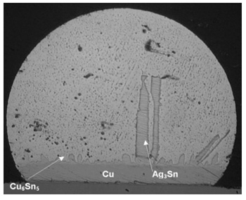
The image to the right is of the Ag3Sn forming as large plates attached to the interfacial intermetallics. This results in plastic strain localization at the boundary between the Ag3Sn plates and the bounding b-Sn phase. xii Adverse effects on the plastic deformation properties of the solidified solder have been reported when large Ag3Sn plates are present.xiii It also has been suggestedxiv that silver segregates to the interface and weakens it by “poisoning”. The brittle fracture is exacerbated by gold contamination.xv
Studies have shown that tin-silver-copper alloys with a low silver content do not experience the growth of these plate-like, Ag3Sn structures, regardless of cooling rates. This suggests that low silver content tin-silver-copper alloys may present fewer reliability issues than other tin-silvercopper alloys.
Conclusion. Evidence from Europe, North America and Japan indicates that the majority of the electronics industry is moving towards the tin-silver-copper family of alloys for lead-free soldering. However, as with any process, care must be taken to select the most appropriate alloy for a broad range of applications. Furthermore, the logistics and economics of specifying a particular alloy must be considered. As pointed out earlier, silver is the cost element in the tin-silvercopper alloys. Since the testing discussed in this paper showed no advantages in terms of processing, reliability, or availability for the high-silver alloys as compared to the low-silver alloys, it is only logical to utilize the less expensive of these for all soldering applications. In fact, the low-silver alloys may have less patent issues associated with them in many parts of the world, as well as superior wetting and fewer reliability issues. As previous reports have shown, it is logical from both a procurement and reliability point of view to utilize the same alloy for SMT, wave soldering, and hand soldering operations.xvi Because the Sn96.5/Ag3.0/Cu0.5 alloy provides manufacturers with the advantages of the tin-silver-copper family of alloys but is less cost-prohibitive than the other alloys tested, individual companies are encouraged to perform further tests in order to determine the viability of this alloy with their particular parts, processes, and applications.
ACKNOWLEDGEMENTS
We would like to acknowledge and thank Kevin Pigeon, International Technical Support Manager of AIM, for PCBA print and reflow test preparations.
REFERENCES
i Nimmo, Kay, SOLDERTEC at Tin Technology Ltd. “Second European Lead-Free Soldering Technology Roadmap (February 2003) and Framework for an International Lead-Free Soldering Roadmap (December 2002)”.
ii Senju Corporation patent # 3027441.
iii Lee, Ning-Cheng, “Lead-Free Soldering- Where the World is Going”. Advanced Microelectronics, pp. 29-34, September/October 1999.
6 Based upon published cost of metals and US$/Euro exchange rate of June 5, 2003
v Whiteman, Lee. “Issues And Solutions To Implementing Lead Free Soldering”. May 2000.
vi Testing performed was the AIM 24 Hour - 15 Board Challenge. Contact the author for a full description of the test procedure.
vii Sohn, John. "Are Lead-Free Solder Joints Reliable?" Circuits Assembly, June 2002, p. 31.
viii Kariya, Yoshiharu and Plumbridge, William. “Mechanical Properties of Sn-3.0mass%Ag-0.5mass%Cu Alloy”. Materials Engineering Department, The Open University, UK.
ix Contact the author for test procedures.
x Seelig, Karl and Suraski, David. ”Advanced Material and Process Issues Lead-Free Electronics Assembly”. April 2001.
xi Henderson, Donald et al. “Ag3Sn Plate Formation in the Solidification of Near Ternary Eutectic Sn-Ag-Cu Alloys”.
xii D. R. Frear, J. W. Jang, J. K. Lin and C. Zhang. “Pb-Free Solders for Flip-Chip Interconnects”. JOM, vol.53, No.6 ( June 2001).
xiii K. S. Kim, S. H. Huh and K. Suganuma, "Effects of Cooling Speed on Microstructure and Tensile Properties of Sn-Ag-Cu Alloys". Osaka University, Japan.. August 2002.
xiv D.R. Frear and P.T. Vianco, “Intermetallic Growth Behavior of Low and High Melting Temperature Solder Alloys,” Metall. Trans. A, 25A (1994), pp. 1509–1523.
xv M. Harada and R. Satoh, “Mechanical Characteristics of 96.5 Sn/ 3.5 Ag Solder in Microbonding,” IEEE Trans. on Comp, Hybrids, and Manuf. Tech., 13 (4) (1990), pp. 736–742.
xvi Seelig, Karl and Suraski, David. “Finally! Practical Guidelines for Achieving Successful LeadFree Assembly”. APEX 2003 proceedings.


