By Karl Seelig, Vice President Technology and Kevin Pigeon, Senior Applications Manager
Introduction. Over the last several years, the electronics assembly industry has witnessed a seismic shift toward component miniaturization. Consumer demands for more functionality in smaller packages have motivated OEMs and Contract Manufacturers to engage in new and innovative technologies. As technological advances usher in a more compact design, a decrease in available board space and more densely populated PCB’s have become increasingly common. In response to these demands, the industry has witnessed a proliferation of Quad Flat No Leads (QFN) packages. The goal of this study is to identify the advantages and challenges that the QFN package brings to the electronics assembly process. This paper will also discuss the results of data evidencing the fundamental steps required to successfully implement QFN technology into an assembly.
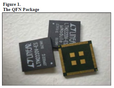
The QFN Package. The QFN package, pictured in (figure 1), is a flat plastic package with perimeter leads underneath the device and larger pads in the center. Its appeal is its compact size and slim body type. It is a small contained package with a near chip-scale sized footprint. It bears a thin body making it ideal for applications where assembly thickness is a consideration. The QFN offers excellent thermal and electrical performance and utilizes perimeter pads to ease circuit board trace routing. These traits make the QFN an optimal choice for many situations where electrical performance, weight, and size are determining factors.
The Challenges of QFNs. Although these cutting-edge devices provide many benefits, they also pose several significant manufacturing and reliability concerns. Defects such as shorts, voids, opens, and deficiencies often make assemblers weary of adopting this new technology. While possessing many appealing features, the QFNs design is prone to voiding on the ground pad. When combined with a lead-free process, the issue of void formation becomes even more of a challenge.
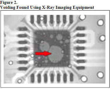
Voiding in QFNs. Voiding in QFNs occurs readily as volatiles become entrapped underneath the pad upon reflow. Unlike Quad Flat Packs (QFPs), QFNs contain no leads and therefore no standoffs to allow for stress absorption and volatile escape. As illustrated in (figure 2), an x-ray imaging system revealed large lake-like voids typical of a QFN ground pad. Due to the enhancement of digital x-ray systems, particularly the transition from analogue to digital detectors, a much clearer,more precise investigation can be performed.
Causes of Voiding. One major cause of voiding in a QFN is component floating. The ultra-small QFN package is designed with a large metal contact pad in the center. When solder paste is printed over this entire pad, or if the thickness of the paste is excessive, there may not be sufficient component weight and/or surface tension to pull the component down to the surface of the board, leading to part floating (figure 3).
When the center pad aperture is large, the paste deposits in this area may be higher than the smaller pads along the edges of the QFN. With the paste deposits in the center being too high (relative to the perimeter pads), the component may not solder to the edge pads (figure 3). This increased volume of solder in the center may also cause the QFN to tilt to one side during reflow and pull out of the opposite side leaving an open along the edge which results in the lifting of the component.
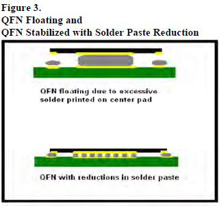
While this is essentially component floating, it often is mistaken for Head-in-Pillow. To prevent component floating, it is necessary to reduce the volume of solder paste printed on the center pad of the QFN to less than 100% coverage.
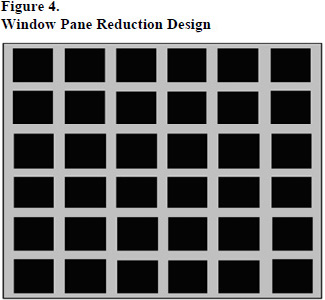
The stencil aperture should be broken down into a series of smaller pads, which reduces coverage from between 50-80% of the pad area. This will not only reduce floating of the device, but also the potential for voiding, splattering, and out-gassing. Guidelines for stencil aperture reduction are further discussed in this paper.
Methods to Minimize Voiding: Adding Vias. The best method of alleviating ground pad voids is modification within the design stage. In many instances, adding via to the pad and/or making a divided, grid-type ground pad will reduce voiding. The via will allow for outgassing of volatiles reducing the formation of voids.
Unfortunately, this option is not available to most contract manufacturers as board design has been fixed and cannot be modified. Since profiling alone has minimal impact on voiding, modifications in aperture reduction, aperture (stencil) design, stencil thickness, and placement/pad design are options.
Aperture Reductions. A variety of designs and percent reductions were utilized to test the effectiveness of decreased aperture size. The most consistent and overall favorable results were achieved utilizing a 30-50% reduction with a window pane reduction design (figure 4) versus 100% coverage. Typical solder paste coverage prior to reflow was 50-80%. Reduction designs may be dependent on the type of assembly being manufactured. It may be necessary to mask or plug vias in order to prevent solder from flowing inside the via during reflow. Another strategy that can be employed is a grid of solder mask on the ground pad that contains voids and allows for some outgassing.
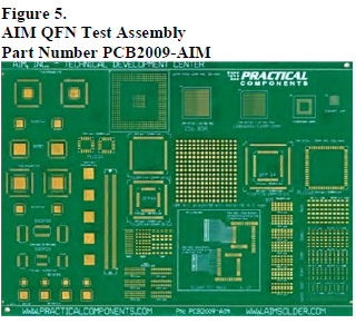
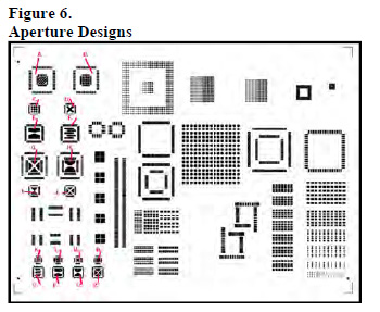
Pictured below in (figure 5) is the AIM Technical Development Center QFN Test Assembly Part Number PCB2009-AIM, which was designed in partnership with Practical Components. The corresponding illustration in (figure 6) shows various aperture designs that have been tested and show positive results in reducing large lake-like voids.
Based on the statistics shown below in (figure 7), some aperture designs have a bigger impact than others. There is not a direct relationship between the percent reduction of paste deposit and voiding. It appears that paste reduction and specific geometries have a positive effect on voiding volume and shape.
Aperture based on percent of paste compared to 100% is:
| A. 57.26 | I. 58.82 | Q. 42.96 |
| B. 47.14 | J. 56.78 | R. 43.20 |
| C. 85.62 | K. 77.80 | |
| D. 84.06 | L. 76.93 | |
| E. 38.10 | M. 75.76 | |
| F. 52.97 | N. 78.10 | |
| G. 59.08 | O. 48.69 | |
| H. 46.79 | P. 34.85 |
Note: Aperture design with proper reduction and geometry helps to eliminate voids. There is a large variation in volume of solder paste on these different geometries.
- E. 38.10%
- F. 52.97%
- I. 58.82 %
- M. 75.76 %
The resulting chart below (figure 7) shows the percentage of the void identified to each aperture change.
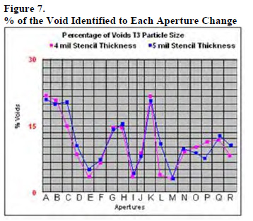
Stencil Thickness. It was determined in most cases that a 4 mil stencil offered significant improvement in voiding over a 5 mil stencil. Nevertheless, it is important to note that reducing stencil thickness can have a negative impact on solder connections on the I/O pads.
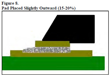
Placement and Pad Design. Even and consistent placement pressure as well as depth is imperative to successful QFN soldering. The component should be under tension on all sides to aid soldering. Moving the pads slightly outward 15-20% will help
maintain tension and allow for some outgassing (figure 8). Pads should not be “necked down” (narrowed) under the component for single row QFNs. This will allow for proper flow and ensure that the traces do not fail during thermal cycling.
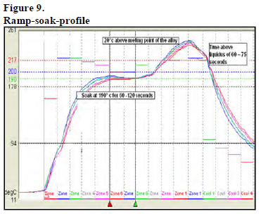
Profile. QFN packages require cooler profiles to reduce voids in the large thermal pads. It is recommended that a straight ramp-to-spike or a ramp-soak-spike profile be used. When using the ramp-soak-spike, a 30-second soak (and a total time to the center of the spike maintained at 3-3.5 minutes) is required. These profiles are very useful when aperture designs have not been incorporated or when mask defined pads are not being used. However, when the boards also contain BGA, there can be a problem. BGA components require long hot soaks and longer profiles. A good profile for void reduction on a BGA runs a soak from 190-200°C for 60-90 seconds and a maximum spike temperature of 235°C. The dwell time above liquidus is 60-75 seconds. This profile can be seen below in (figure 9). When balancing a profile, it is important to consider both components.
CONCLUSION. Since “small” is the only option for many of today’s designers, the QFN package will continue to make its way into the modern day world of electronics. The geometry of this package brings appeal in the form of excellent thermal and electrical integrity. Conversely, several manufacturing considerations cannot be overlooked. The issues discussed in this paper reference the major concerns and potential remedies required to increase reliability and reduce defects.
If strategies can be employed during the design phase, adding a via to the center pad and/or making a divided gridtype ground pad would be most beneficial.
Paste selection can have an impact, but the nature of what occurs during solder paste reflow is unavoidable, irrespective of paste formulations. Where there is a large solder pasted pad under a component with no room for outgassing, voiding will occur.
Other possible modifications in order of impact include:
- Stencil Aperture Design. When designing your pattern, the pattern must offer capillary action of the solder gasses to the edge of the ground plane. This can be successfully accomplished by using patterns with enough space and flow lanes to create movement outwards from the center of the pad.
- Solder Pad Mask Defined Grid. Keep in mind, if a solder pad mask grid is being used, voids are often present. The grid eliminates lake voids and keeps voids more dispersed, therefore eliminating hot spots. The down side is that grid defined pads can lead to failures in harsh environments. This is due to the thermal expansion of the mask against the solder.
- Paste Powder Distribution. It is known that finer particles tend to void less on BGA’s and other types of solder connections.
- Paste Volatility & Wetting. Increased wetting can help. This will affect the speed of the capillary flow by moving more gas to the edge of the pad.
With any evolving technology, more testing is required to further grasp the issue of voiding activity in the QFN package.
REFERENCES
1) D. Bernard, B. Willis, M. Morrell & M. Beadel. Analysis of Voiding Levels under QFN Package Central Termination and their Correlation to Paste Deposition Volumes and Propensity for Device Stand-off and Poor Joint Quality. Presented at IPC Event. 2011.
2) B. Toleno. Increased Use of QFN’s Brings Challenges to Light. Dataweek. 23 July 2008.