By Tim O’Neill
This technical article explores an unconventional yet promising technique for reducing QFN voiding in surface mount technology (SMT) manufacturing. By shifting the focus from the ground pad to the I/O (Input/Output) pads of the QFN package, this method not only offers a fresh perspective on mitigating voiding issues but presents a cost-effective solution without adding complexity to the solder assembly process.
Introduction to QFN Voiding Challenges
Integrating Quad Flat No-lead (QFN) packages into solder assembly processes often results in a persistent challenge: voiding.
Voids or air pockets within the solder can compromise the thermal and mechanical reliability of the solder joint. This is particularly critical for QFNs, which are commonly used in high-performance and high-reliability applications.
Traditional efforts to mitigate QFN voiding involve modifying reflow profiles, refining solder paste formulations, and experimenting with different stencil designs and aperture sizes. These stencil aperture design modifications usually focus on the ground pad. While these methods offer some success, they also require significant alterations in the manufacturing process, leading to increased complexity and costs. Moreover, the persistent nature of QFN voiding indicates that a more innovative approach is necessary to address this issue effectively.
In the following sections, we look at a novel approach which involves modifying the I/O pad stencil apertures. We outline the experimental methodology used to test this approach, the results observed, and the theoretical implications.
Experimental Methodology
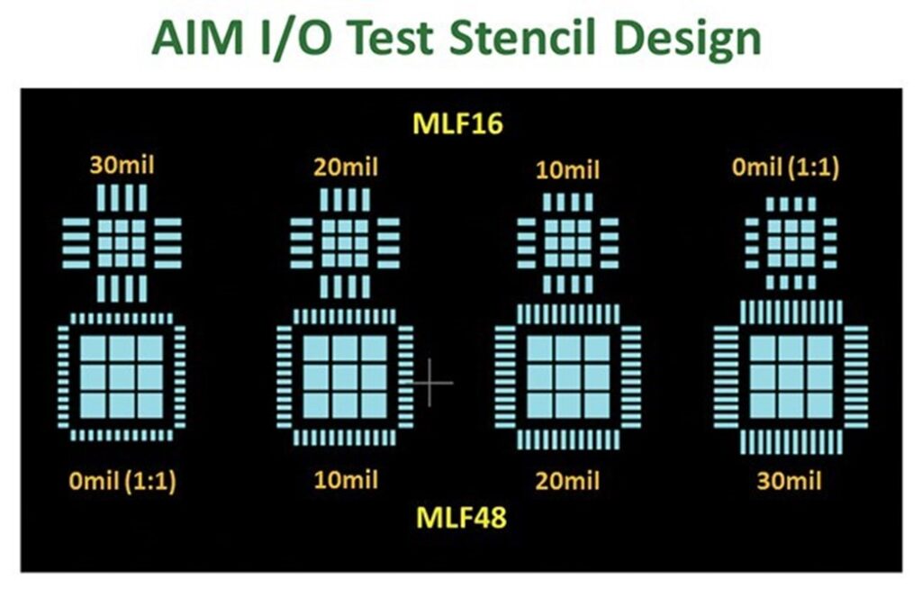
The study focused on three distinct Micro Lead Frame (MLF) devices: MLF16, MLF32, and MLF48. For each of these MLF devices, four distinct I/O pad print patterns were tested:
- A 1 to 1 print, which matched the I/O leads exactly, serving as the baseline for comparison.
- An overprint extending the print by 10 mils beyond the I/O leads.
- An overprint extending the print by 20 mils beyond the I/O leads.
- An overprint extending the print by 30 mils beyond the I/O leads.
This choice of print pattern variation was informed by previous incidental observations of reduced voiding with I/O overprint. It was hypothesized that these small increments in overprint (10, 20, and 30 mils) would effectively pull back during the reflow process and we could determine any associated effects on voiding. Figure 1 shows examples of the stencil design for this experiment.

Type 4, no clean SAC305 solder paste was printed through a 4mil (100μm) premium stainless-steel stencil with a fluoropolymer nanocoating on PCB2009 test boards. A ramp-to-spike, or linear, profile was used.
Most void reducing reflow profiles incorporate prolonged thermal exposure or soak zones to promote flux volatilization prior to the alloy reaching liquidus. Since the goal of this study was to isolate and assess the efficacy of the I/O overprint, we chose the least forgiving thermal profile. X-ray results were then analyzed both visually and with statistical software.
Observations and Results
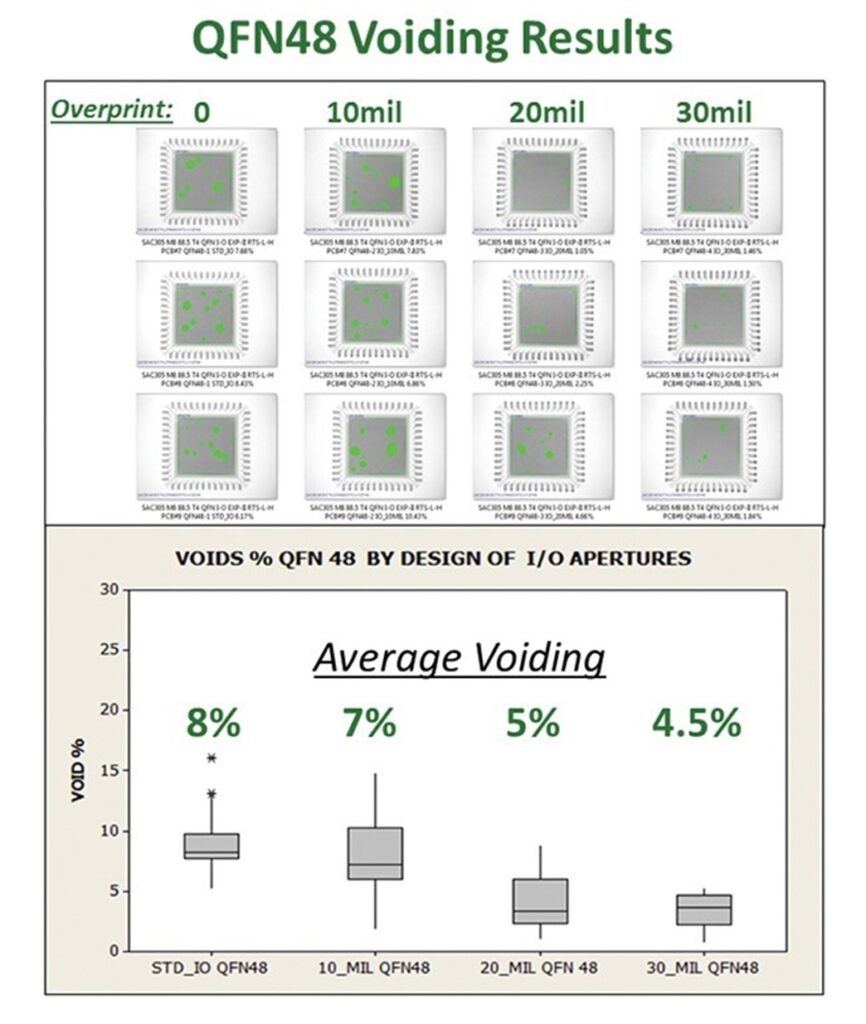
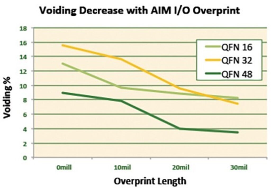
The QFN packages with modified I/O pad apertures exhibited a consistent decrease in void formation with larger I/O overprinting. On average, there was an over 50% reduction in voiding across various device types and sizes from the 0mil baseline to the 30mil samples. This is clearly visible in Figure 2, which shows the voiding results for MLF48.

Figure 3 further highlights the comparative analysis of voiding in traditional vs. modified pad designs. Regardless of size or configuration, the I/O pad modification approach demonstrated a uniform effectiveness in reducing voiding.

These study results validate the effectiveness of I/O pad modification as well as open new avenues for solder assembly process optimization.
Proposed Explanation of the Results
The following proposed explanation is hypothetical and has not been experimentally confirmed, but we believe it provides a plausible description of the mechanisms behind these remarkable results.
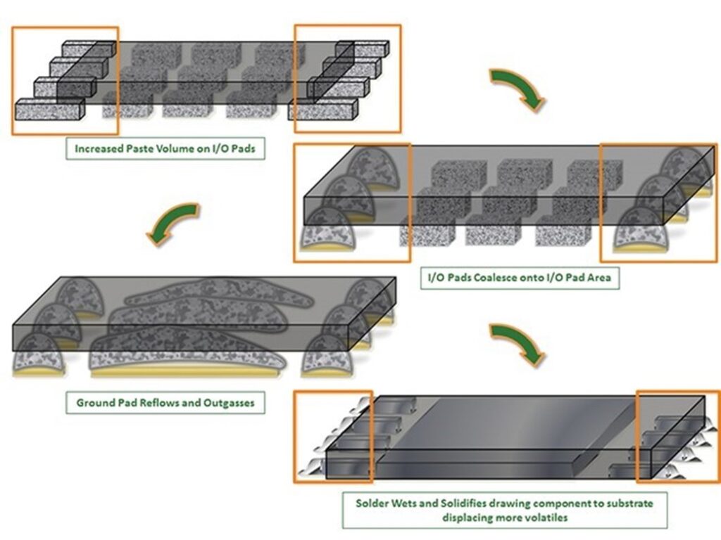
Because the I/Os are on the perimeter, they reach liquidus temperature before the center pad. As they melt, the overprints coalesce onto the I/O pads. This lifts the component for a brief period – the time between the outside melting and the inside melting.
As soon as the print on the center pad melts and wets, the package collapses the solder. That momentary lifting may be enabling rapid outgassing and/or the collapse of the component itself may force gas out as it compresses the liquid solder. This process is illustrated in Figure 4.

Implications and Future Research Directions
The demonstration that minor modifications to I/O pad stencil apertures can lead to a significant reduction in voiding presents a potential paradigm shift in QFN soldering techniques. Manufacturers can adopt this approach with minimal disruption to existing processes, as it does not require new equipment or materials.
While the study focused on specific QFN types and conditions, future research could expand the scope of this approach. Explorations could include varying solder paste types, different reflow profiles, and other package types. Additionally, long-term reliability studies would be beneficial to understand the impact of these modifications over the lifespan of electronic devices.
Based on the article “Aperture Design to Minimize QFN Voiding” by Tim O’Neill, originally published in Circuits Assembly.


