by Timothy O’Neill and Logan Jelinske
Abstract
Despite predictions of the demise of through-hole components, they remain commonplace throughout the industry. However, their use is in decline and assemblies may only incorporate one or two through-hole components. An alternative technique for soldering through-hole components, eliminating the need for a separate soldering process, is the Pin-in-Paste (PiP) or Intrusive Reflow method. PiP utilizes solder paste printing and the SMT reflow processes to solder through-hole devices. The PiP technique can be more cost effective by eliminating the need for a wave or selective soldering process and the associated costs. This paper will detail the PiP process including PCB and stencil design considerations as well as solder paste selection and reflow guidelines.
Background
As electronic devices continue to become smaller and more capable, through-hole components are implemented less often, with space constraints of modern devices the driving force. However, through-hole devices offer performance advantages over SMT as they have robust interconnections with compliant leads that increase mechanical and electrical reliability. PiP soldering can provide equivalent process and product performance to wave, selective and hand soldering during SMT assembly, thus reducing cost. Operating a wave or selective solder machine can be costly and the additional process step can be eliminated. PiP can also eliminate the need for underutilized equipment and increase space on the production floor.
PiP Considerations
Considerations for PiP implementation using through-hole components are:
- Components are verified to be capable of withstanding SMT process temperatures and the method of insertion established. After the solder paste is printed, the components can either be placed manually or by automated insertion.
- The component must have adequate clearance to prevent solder contacting the bottom of the component, a defect per IPC-610G 7.3.5.
- Lead to hole ratio needs to be as tight as is practical. A large lead to hole ratio will result in an increase in paste volume, voiding and the potential for solder to flow out of the through-hole during reflow. Too tight of a lead to hole ratio will result in insufficient barrel fill and insertion issues.
- Lead length should be kept as short as possible. Excess lead length will displace paste on insertion and can wick solder away from the barrel increasing the need for solder volume.
Paste volume requirements to achieve adequate barrel fill must be balanced with SMT requirements to prevent bridging/shorts etc. Solder paste on-mask/over-print is an accepted technique for increasing paste volume but it is limited by component spacing and other board features. Additionally, the diversification of alloy options may impact/reduce wetting force and pull-back required for overprinting to be effective.
Step stencils may be implemented to achieve adequate barrel fill without adversely impacting other solder joints. Advancements in solder stencil micro-welding techniques have eliminated many of the inconsistencies associated with earlier technologies. Jetted solder paste is a recent development that provides a non-contact means of increasing local paste volume. Solder preforms can also be utilized to increase solder volume.
Minor process adjustments can be made to increase barrel fill by experimenting with printer settings including off-contact printing, manipulating squeegee speed, pressure, angle of attack and stroke count.
Solder Joint Volume Calculation
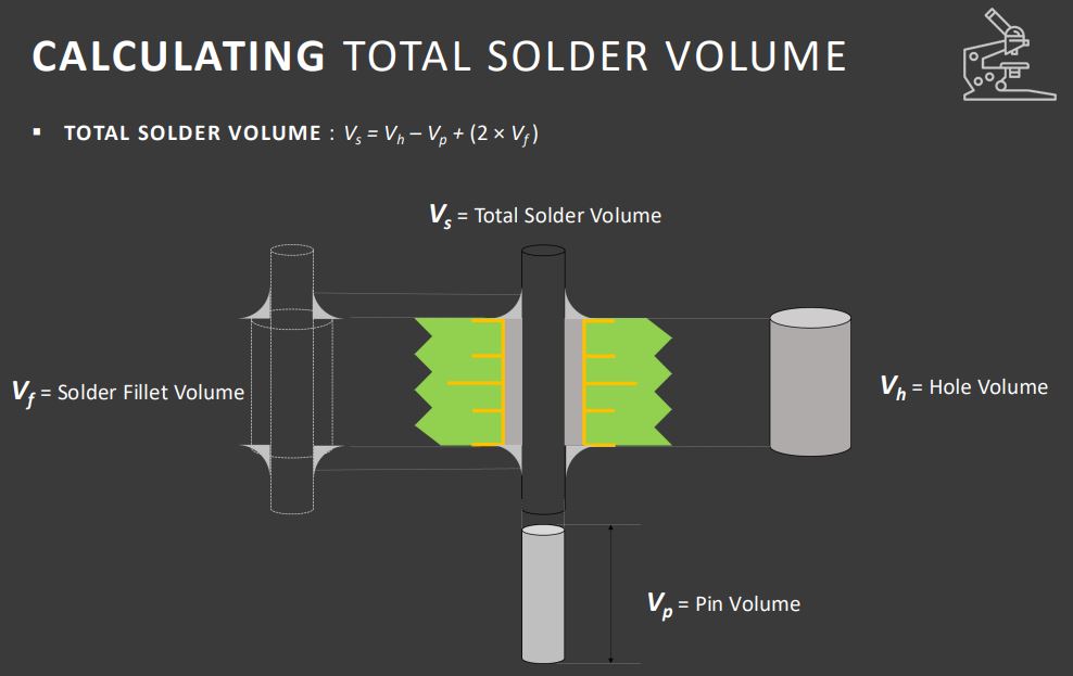
The required solder joint volume, Vs, is calculated by the difference of the volume of the through-hole and the volume of the pin. The formula is:
Solder Joint Volume = Volume of Through-Hole – Volume of the Pin + (2 x Solder Fillet Volume)

This formula will account for the amount of solder needed to ensure proper through-hole barrel fill. For the volume of the through-hole, Vh:
Vh = πRo2H
Where Ro is the radius of the through-hole and H is the height of the through-hole or the thickness of the PCB. The volume of the solder fillet, Vf, can be calculated using the following formula, derived from Pappus’ Centroid Theorem:
Vf = 2πA(0.2234R2 + Rt)
Where fillet radius, R, is equal to the difference in the radius of the pad and the radius of the pin (R = Rp-Rt). Fillet area, A, is equal to 0.215R2. To calculate the volume of the pin, Vp:
Vp = πRt2H
Once Vh, Vf, and Vp are calculated, the solder joint volume formula reduces to the following:
Vs = Vh – Vp + (2 x Vf)
Since, solder paste is approximately 50% solder by volume, a reduction factor, F, is needed to determine the amount of solder paste needed. The reduction factor is generally between 0.45 and 0.55 depending on the solder paste formulation. The formula to calculate the volume of solder paste, Vsp, is:
Vsp = Vs/F
Stencil Apertures
Once the volume of solder paste is determined, the next step is to design the stencil used for the process. For a general circular aperture design, use:
Vsp = πr2t
Where r is the radius of the aperture and t is the thickness of the stencil. For a general rectangular aperture, use:
Vsp = lwt
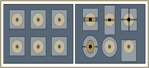
Where l is the length, w is the width, and t is the thickness of the stencil. Use arithmetic to adjust the radius for circular apertures or length and width for rectangular apertures to meet the necessary volume of solder paste required, Vsp. Depending on the required application, different aperture shapes may be beneficial. As seen in Figure 2, various aperture shapes and sizes may be used to increase performance during the process.

PCB Considerations
The primary objective of a PiP process is to create a quality solder joint. There are a several PCB considerations that can ease implementation.
The pad surrounding the barrel should be as small as possible while maintaining adequate mechanical properties. In general, this is 2x the plated barrel diameter. This has the benefit of reducing the paste required fulfilling the IPC-610G 4.3.2.1. standard.
Another PCB consideration is the lead to hole ratio. As previously mentioned, this should be kept as small as possible but it should account for tolerances with the connector and PCB to allow for variation in placement accuracy while requiring minimal insertion forces.
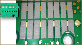
In order to fulfill the solder volume requirement for a PiP process, printing solder paste on to the PCB solder mask is necessary as seen in Figure 3. Overprinting on the solder mask may be limited by the space and location on the PCB. The solder mask and pad surface finish can have a significant influence on result. Solder mask with high surface energy will keep the molten solder flat, where solder reflowed on mask with a low surface energy will tend to bead and can interfere with the component while liquidus due to a high wetting angle. The solder mask should also be applied to exposed copper to ensure molten solder flows into the barrel and all non-test vias should be tented. Additionally, easily solderable surface finishes such as HASL and ENIG will promote wetting and improve results.

Solder Paste Selection
A key variable in PiP soldering is the solder paste in use. There are a number of paste properties that can have a strong influence on the success of PiP soldering. Some of the most significant are hot slump performance, wetting performance, alloy type and residue characteristics. Solder paste hot slump is tested per IPC TM-650 2.4.35 Sec. 5.2.2. This test quantifies the ability for a solder paste deposit to resist deforming at 150°C for 10-15 minutes. This is a significant property as paste that can resist slumping is less likely to fall through and out of the barrel prior to becoming liquid. Solder paste with better wetting properties will improve process capability and can overcome some of the aforementioned issues. Flux chemistry and alloy can impact wetting performance. For example, as low temperature alloys are investigated, the impact of wetting properties on PiP performance should be evaluated.
Reflow Considerations
The solder paste reflow profile can be manipulated to impact the outcome of solder joint quality for the entire PCB assembly, not just the PiP component. There are a number of considerations when making profile adjustments to achieve the best possible outcome. The most common constraining factors when developing a reflow profile include solder paste recommendations, component temperature limitations, assembly thermal mass characteristics, oven capability and limitations. The profile used must accommodate these constraints while satisfying the application quality objectives.
Quality Assessment
PiP solder joint quality should meet IPC-610 criteria for Class 1, 2, and 3. Non-destructive X-ray and destructive cross-sectioning can provide definitive evidence regarding whether the process is successful.
Downstream Processes
Incorporating a PiP process can have unexpected implications for a number of post reflow processes. As solder paste is 50% flux by volume, adding additional paste to the PCB to accomplish barrel fill can significantly increase the amount of post soldering flux residue. Keep in mind that liquid flux used in wave and selective soldering leave very little residue. Increased solder paste residue can cause a number of issues:
- Aesthetic – Simply put, increased flux residue is not visually appealing.
- ICT – Increased flux residue can interfere with test probes contacting the test area leading to ‘false calls.” Increased test fixture maintenance, probe replacement and cleaning may be required.
- Reflow Oven – Increased paste leads to increased flux volatiles being generated during the reflow process. This results in flux residue accumulating in the oven causing increased cleaning of flux management system and flux dripping in the reflow oven. Additionally, paste displaced from the barrel during the insertion process can fall off the tip of the pin and accumulate in the bottom of the reflow oven.
- Flux residue and/or solder paste can flow to the end of the connector which can violate quality standards or interfere with clearance and tolerance limitations.
Conclusion
Through-hole components continue to be commonplace and it is unlikely they will be eliminated in the foreseeable future. Modern day assemblers are constantly adopting new processes and optimizing existing processes. It has been proven that PiP can help reduce operation costs, simplify the production process, reduce the assembly line footprint and save energy. As new alloys, smaller devices and new technologies are incorporated PiP remains a useful technique to the PCB assembly industry.


