As the electronics industry pushes the boundaries of miniaturization, the precision of solder paste printing has taken center stage in the manufacturing process. This evolution demands not only meticulous technique, but a deep understanding of ultrafine solder paste properties.
Drawing on the knowledge of our process engineers, metallurgists, and chemists, this article aims to provide a comprehensive understanding of the challenges, innovations, and best practices that define this specialized field.
Understanding Solder Paste Powder Sizes
Solder paste is classified by its powder size, with Types 3, 4, 5, and 6 currently being the most common in the industry. Each powder size has unique properties that influence aspects such as printability, reflow behavior, and overall assembly performance.
Ultrafine solder pastes are those with powder size starting in the Type 5 or Type 6 range and smaller. The following table provides a sense of the relative sizes of solder paste types from type 3 through type 10.
| Powder Type | Smallest Diameter Spheres | Largest Diameter Spheres | Use Cases |
| Type 3 | 25 µm | 45 µm | Ideal for 0402 imperial components. Can print apertures down to 225µm in diameter. |
| Type 4 | 20 µm | 38 µm | Recommended for 0.5mm BGAs, Micro BGAs, and 0201 imperial components. Can print apertures down to 190µm in diameter. |
| Type 5 | 15 µm | 25 µm | Essential for the assembly of QFNs, µBGA, and 01005 devices. Can print apertures down to 125µm in diameter. |
| Type 6 | 5 µm | 15 µm | Suited for print apertures 80 – 150µm in diameter and possibly smaller with careful process control. |
| Type 7 | 2 µm | 11 µm | Innovative applications with ultra-small component sizes. Can print through apertures as small as 55μm. |
| Type 8 | 2 µm | 8 µm | Emerging |
| Type 9 | 1 µm | 5 µm | Emerging |
| Type 10 | 1 µm | 3 µm | Emerging |
Exploring Ultrafine Solder Paste Applications: Micro/MiniLED, Die Attach, and SiP
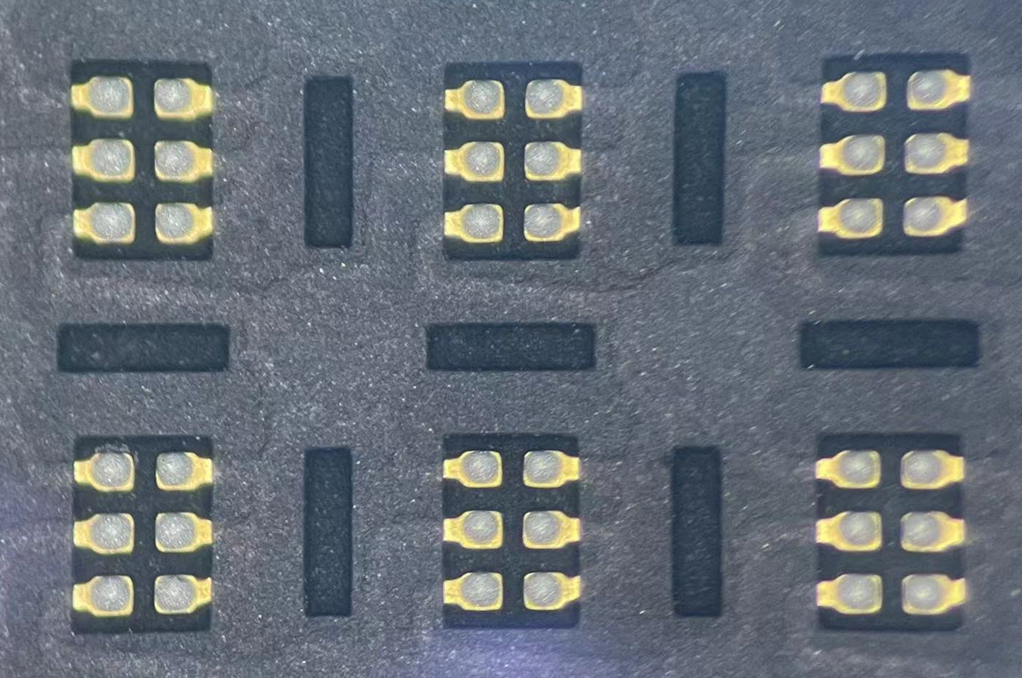
In terms of production and PCB assembly, ultraminiature soldering involves creating solder prints that are less than a millimeter – or even less than a tenth of a millimeter – in diameter. This is achieved using advanced printing techniques that can accurately place and reflow the tiny amounts of solder paste needed.

Because of the small package sizes, the component placement for such applications is equally precise, often necessitating robotic assistance. This precision is paramount, especially when dealing with components like 01005s (0.4mm x 0.2mm), or even 008004s (0.2mm x 0.1mm) and smaller where the margin for error is virtually nonexistent.
MiniLED and MicroLED
Mini and microLED technologies involve assembling tiny LEDs onto substrates for display applications, demanding high precision and consistency. MiniLEDs may be as small as 150 x 100μm, necessitating the use of Type 6 solder pastes. MicroLEDs are an emerging technology and may be 50 x 50μm, requiring Type 7 or finer pastes for accurate and reliable soldering.
Die Attach
Die attach, a critical step in semiconductor packaging, involves bonding a chip to a substrate or leadframe. The solder used is often in the form of paste or preforms, with particle sizes varying based on application specifics. For finer pitch components, smaller solder powder sizes (Type 5 or finer) are used to ensure a precise and reliable bond, with Type 7 pastes required for some of the smallest applications.
System in Package (SiP)
System in Package (SiP) technology integrates multiple electronic components into a single module, optimizing space and performance. They are manufactured through complex assembly processes involving precise placement and soldering of various components, often requiring micro-sized solder balls or paste. The components demand ultrafine solder powder sizes, typically Type 6 or finer, to ensure accurate and reliable interconnections in these densely packed environments.
Technical Challenges and Best Practices for Ultrafine Solder Paste Printing
In ultrafine solder paste printing, engineers confront several technical challenges. For finer powders (Types 5, 6, and beyond), special considerations include:
Stencil Design
The stencil must be thin enough to allow the fine pitch printing required for ultraminiature components but also sturdy enough to withstand the pressures of the printing process. Stencil thicknesses as low as 25μm are not uncommon in this domain.
Employing a “squircle” aperture design, as opposed to traditional circular or square designs, has proven effective in improving paste release and reducing the likelihood of solder defects.
Gasketing
In the ultrafine realm, proper gasketing – the seal formed between the stencil and the PCB – is crucial for preventing solder paste from bleeding or smudging outside the designated pad areas. Ensure the printer’s parameters (squeegee speed, pressure, and separation speed) are finely tuned for the specific type of solder paste used. Since the particles may be as small as 2μm, even a tiny gap could allow leakage. It’s also important to regularly inspect and clean stencils to prevent blockages.
Board Registration
Precise alignment between the stencil and the board ensures that solder paste deposits accurately on the intended pads. Any misalignment, even at a microscopic level, can lead to solder bridging or insufficient solder on pads. This precision becomes even more critical as component sizes decrease and pad proximity increases.
Managing Oxidation
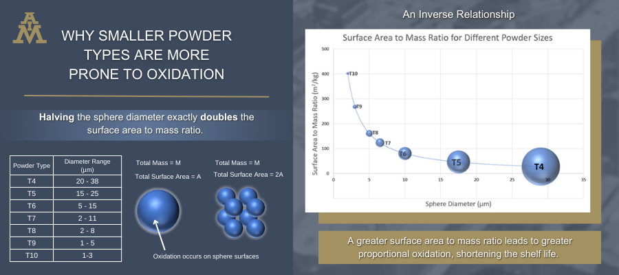
Finer particles have a larger relative surface area, making them more prone to oxidation. The infographic below demonstrates just how much the total surface area of solder powder increases as paste size goes down. Nitrogen is often required, not just recommended, during reflow to minimize oxidation.

Handling and Storage
Ultrafine solder pastes have a shorter shelf life, which requires stringent stock management and application of the first in first out (FIFO) principle. The viscosity of ultrafine pastes also tends to be higher, demanding more meticulous mixing and application techniques to maintain consistency.
Reflow Profiling
Reflow profiling, the process of carefully controlling the temperature profile during solder reflow, must be meticulously managed. Even minor deviations can lead to defects in solder joints, particularly when dealing with components of such diminutive size. Monitor and adjust reflow profiles to suit the specific characteristics of the solder paste, taking into account factors such as flux activity and thermal behavior.
Conclusion
Understanding and mastering ultraminiature soldering is more than a technical requirement; it’s a strategic imperative for staying competitive. As devices continue to shrink and customer demands for performance and reliability grow, the margin for error narrows.
Through the collective expertise of our process engineers, metallurgists, and chemists, we are not just observing these industry shifts; we are actively contributing to them. Contact our technical support engineers today if you need help with implementing an ultrafine solder paste process.


